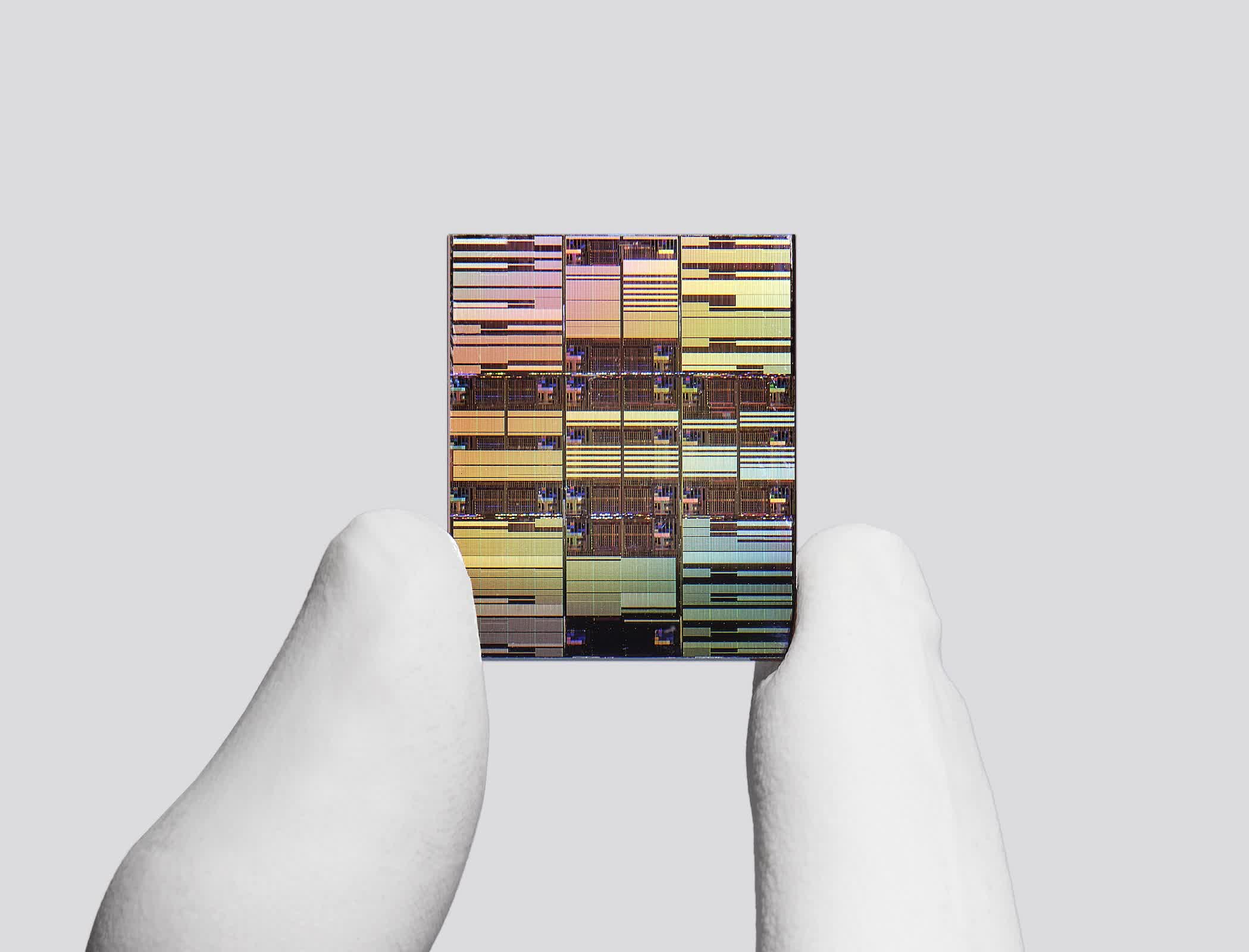
First look: IBM is once again testing the limits of chip design, this time with an architecture that moves beyond traditional scaling into a more three-dimensional layout aimed at AI workloads. The company refers to the design as a "nanostack" architecture and says it can fit nearly 100 billion transistors onto a chip roughly the size of a human fingernail. That's roughly double the density of IBM's last generation, but the bigger story is how it gets there.
Rather than continuing to shrink components along a flat plane, IBM is stacking transistors vertically. That change comes as semiconductor designers run up against the physical limits of traditional scaling, making further miniaturization increasingly difficult and less efficient.
In a media briefing covered by Ars Technica, IBM describes the breakthrough as the "world's first sub-1-nanometer chip technology" for AI data centers, though the label is more about performance expectations than literal dimensions. Node names have not corresponded to physical measurements for years. Here, IBM is basically saying the chip behaves like a true sub-1-nanometer design, even though its physical features aren't that small.
"It's not just an incremental step, it's a meaningful leap forward," said Jay Gambetta, director of IBM Research and IBM Fellow, in the briefing. He described the new chip technology as "pointing to a future where computing becomes significantly more powerful without a corresponding increase in energy."
The architecture builds directly on IBM's earlier work with nanosheet transistors, which formed the basis of its 2-nanometer node introduced in 2021. In the new design, the basic unit consists of two transistors stacked and bonded together. Each transistor is made up of three nanosheets, each about 5 nanometers thick, with roughly 9 nanometers of spacing between them.
That layered structure allows IBM to increase transistor density without relying on further horizontal shrinkage, which has become increasingly impractical. In practice, that means it improves performance by building upward rather than just shrinking features sideways.
The potential impact on AI infrastructure is a central part of the pitch. According to IBM's projections, the nanostack architecture could deliver up to 50% higher computing performance or 70% better energy efficiency compared with its 2-nanometer chips. For data centers already grappling with power constraints, those kinds of improvements are not incremental.

Memory performance is another area where IBM is targeting gains. The company reported a 40% improvement in SRAM scaling, enabled by a staggered-channel design that cuts overall cell height and improves SRAM density. SRAM plays a critical role in AI systems because it supports fast data access, but it has also been one of the hardest components to scale in recent chip generations.
"This achievement of 40% will eventually industrialize itself in AI workflows, which require higher bandwidth and high efficiency," Gambetta said.
The redesign focuses on SRAM bit cells, each made up of six transistors, allowing more memory to fit within the same footprint. That's important because recent node transitions, including the move from 3-nanometer to 2-nanometer technologies, have delivered only modest improvements in SRAM scaling.
IBM's role in all of this remains rooted in research rather than manufacturing. The company typically works with partners to bring its designs to market. It has collaborated with Rapidus in Japan on 2-nanometer production and with Samsung on related semiconductor advances.
At the same time, other major players, such as TSMC, have independently adopted nanosheet transistor designs, reflecting how IBM's research tends to influence the broader industry.
"Nanosheet has become the foundation of the next generation of transistor scaling," said Huiming Bu, vice president of IBM Semiconductors Global R&D and IBM Research. "Today, nanosheet is adopted by all leading foundries for most of the 3-nanometer chips and all of the 2-nanometer chips."
Looking ahead, IBM has not named partners for commercializing the nanostack architecture, but it expects the technology to reach production within the next decade, possibly sooner. Bu said the design is positioned to replace nanosheet architectures as the industry standard across processors, including CPUs and GPUs.
"It will replace nanosheet as today's mainstream in leading foundries, whether it's CPUs or GPUs," Bu said. "Within a decade, this will become another mainstream that we have invented and helped industry to transform."