The takeaway: Intel is betting that advanced chip packaging, not just new process nodes, will power its comeback – and it is now in talks with Google and Amazon about advanced AI chip packaging services, according to multiple sources. Those potential customers, both major builders of custom AI silicon, would test whether Intel's packaging technology can win business away from entrenched foundry rival TSMC and turn its Foundry unit into a meaningful revenue engine.
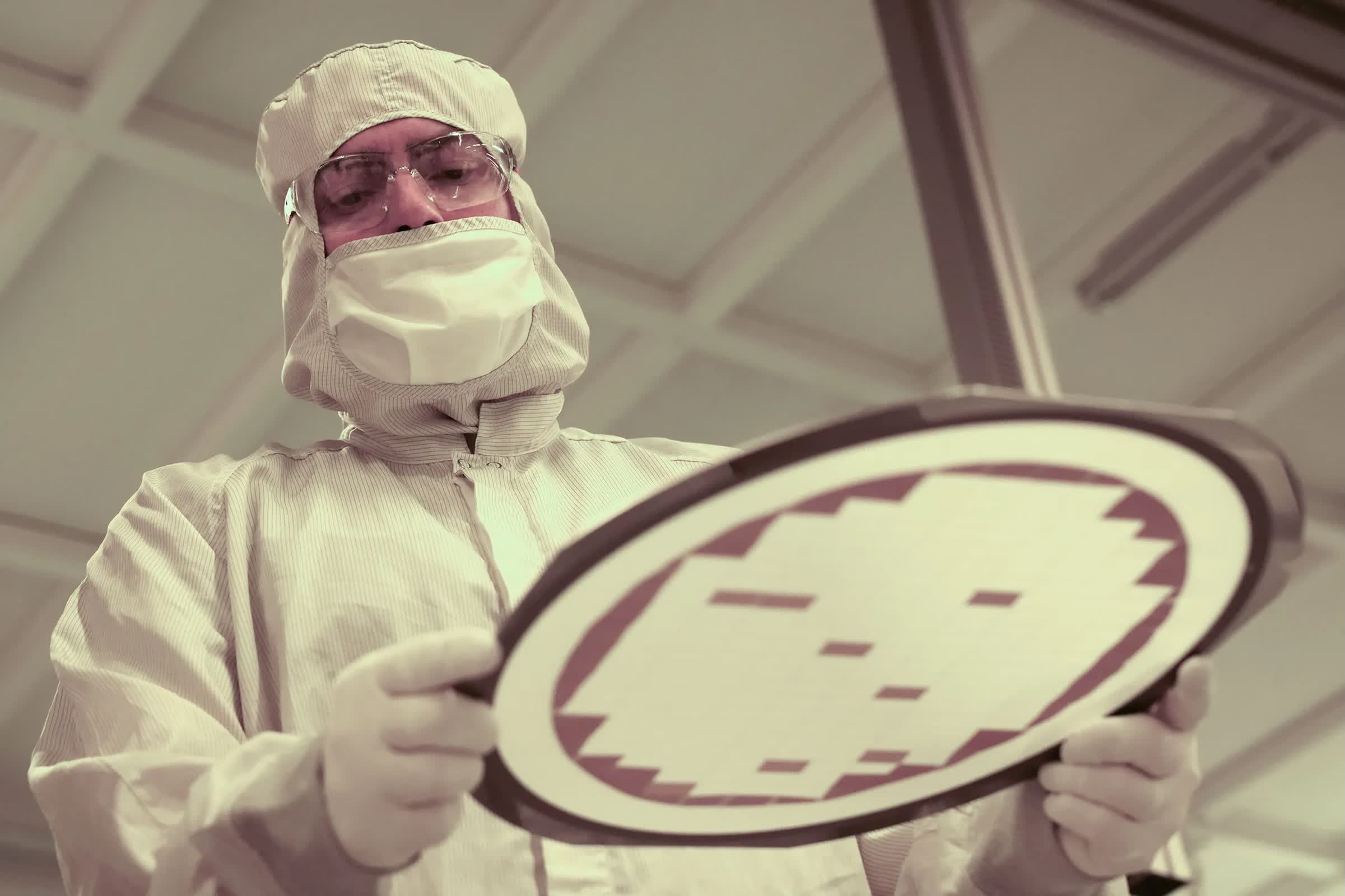
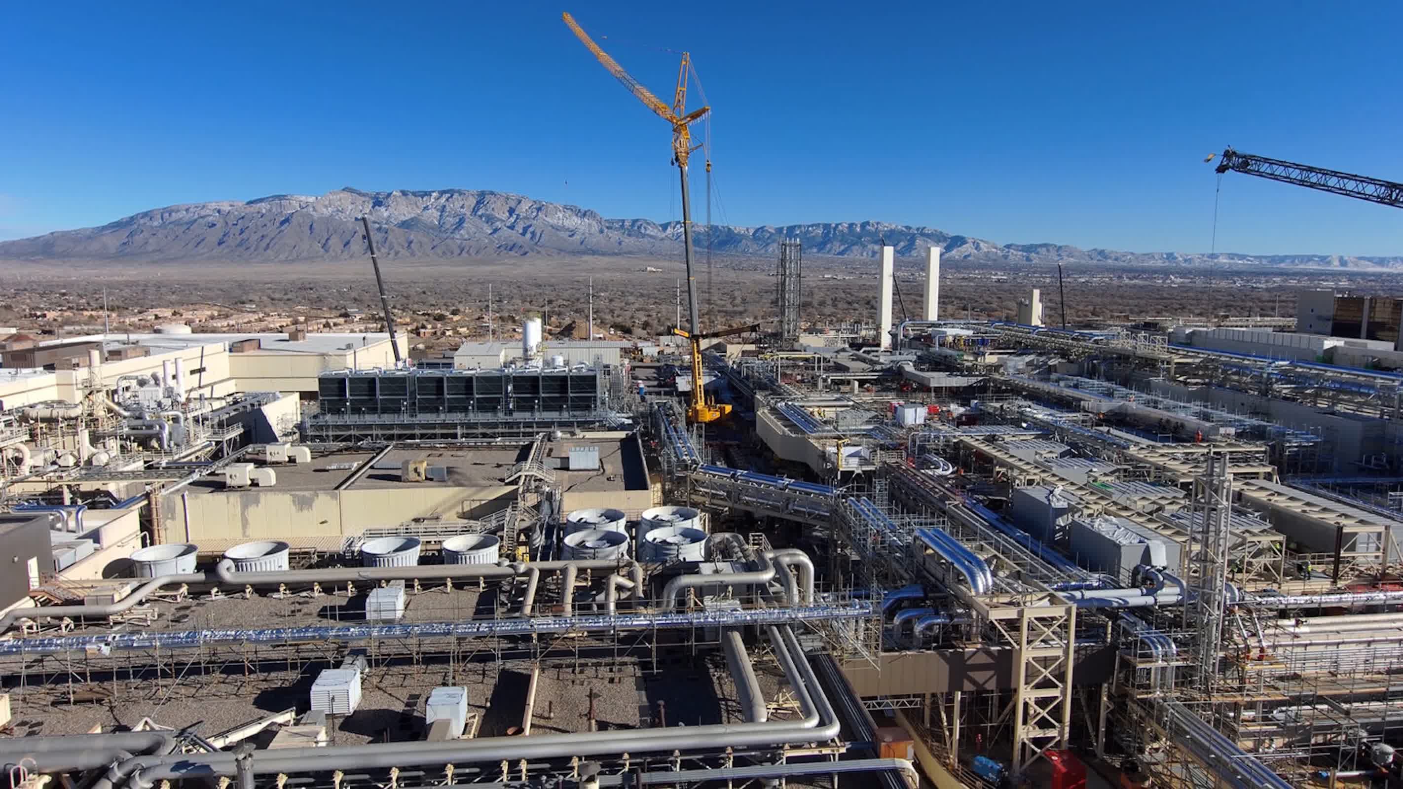
Packaging has shifted from a back-end afterthought to the center of Intel's manufacturing strategy as AI workloads push designers to stitch together many specialized dies into a single system. At its Rio Rancho, New Mexico, site – once home to a shuttered Fab 9 that sat idle for years – Intel has poured billions of dollars, including $500 million from the US Chips Act, into repurposing Fab 9 and neighboring Fab 11X as advanced packaging lines inside Intel Foundry.
Those facilities support technologies such as EMIB and Foveros, which connect multiple chiplets in 2.5D and 3D configurations to squeeze more bandwidth and memory into a single package for AI and data center processors.
Intel's current portfolio focuses on EMIB, which embeds tiny silicon bridges in the package substrate to link chiplets, and Foveros, its 3D die-stacking technology. The next step is EMIB-T, a new version that adds through-silicon vias to the bridge to improve power delivery and signal integrity across densely packed dies. EMIB-T is slated to reach production fabs this year and is designed to support very large AI-class packages up to 120 x 180mm, with room for more than 38 bridges and over a dozen reticle-sized dies, according to technical disclosures.
Internally, packaging has become one of the most closely watched parts of Intel Foundry's model. During a January earnings call, CEO Lip-Bu Tan described the company's packaging as a "very big differentiator" versus competitors, while chief financial officer Dave Zinsner said he expects packaging revenue to "come in even before we start to see meaningful wafer revenue."
Zinsner told investors that his forecast for packaging had been revised over the previous 12 to 18 months from "hundreds of millions of dollars" to "well north of $1 billion." He later called packaging "ironically, the more interesting part of the Foundry business today," adding that Intel was "close to closing some deals that are in the billions of dollars per year, in terms of revenue on packaging."
Zinsner also said he believes Intel Foundry's packaging business can reach gross margins of about 40%, in line with the rest of its products.
Those deals are understood to involve hyperscale cloud providers. Multiple sources have told Wired that Intel has been in ongoing talks with at least two large customers for its advanced packaging services: Google and Amazon, both of which design custom chips but outsource significant parts of their fabrication and assembly.
Google spokesperson Lee Fleming declined to comment, saying the company does not publicly discuss supplier relationships. Amazon also declined to comment, and Intel said it does not comment on specific customers.
Since 2024, Intel has effectively operated as two businesses: a long-standing product side that designs and sells CPUs to PC makers and data centers, and the Foundry unit that manufactures advanced semiconductors and offers packaging services. Naga Chandrasekaran, head of Intel Foundry, told Wired that the very idea of "advanced packaging" is relatively new and that AI has pushed it to the forefront. "Because of AI, advanced packaging has really come to the forefront," he said. "Even more so than the silicon itself, chip packaging is going to transform how this AI revolution comes to fruition over the next decade."
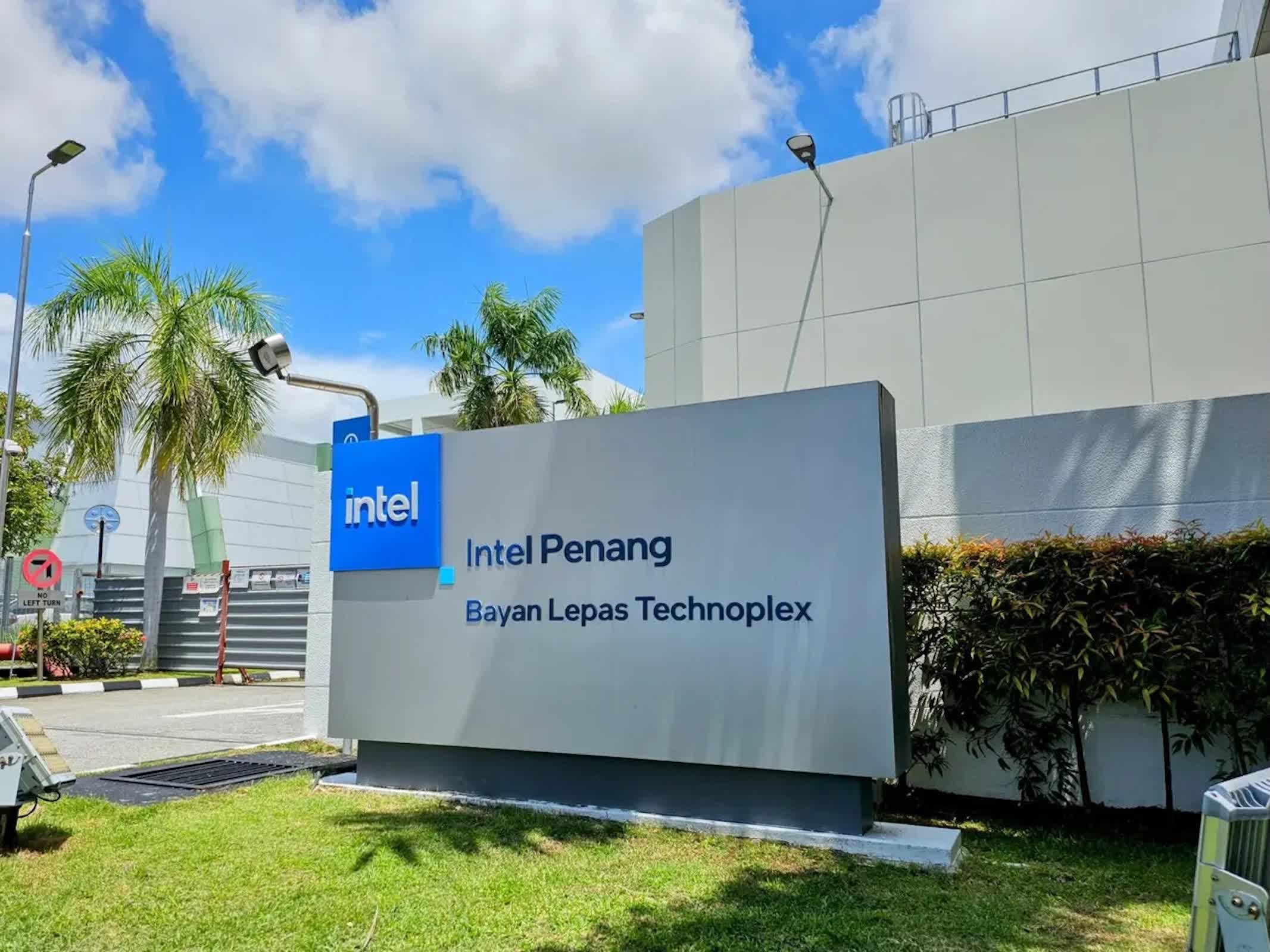
To support that vision, Intel is expanding capacity well beyond New Mexico. Malaysian Prime Minister Anwar Ibrahim said in a Facebook post that Intel's Penang advanced packaging complex, originally established decades ago, is now entering a new expansion phase that includes advanced packaging and is expected to begin its first-phase operations later this year. "I welcome Intel's decision to begin operations for the complex later this year," Ibrahim said in the translated post, after a briefing in which he said Intel Foundry head Naga Chandrasekaran had "outlined plans to commence the first phase" of the build-out.
– Anwar Ibrahim (@anwaribrahim) December 1, 2025
Intel spokesperson John Hipsher confirmed that the company is adding chip assembly and test capacity in Penang "amid rising global demand for Intel Foundry packaging solutions."
Chandrasekaran has suggested that investors will see the impact of any large outside wins not through customer lists but through Intel's spending patterns. He said the big indicator that customers have signed on will be a noticeable jump in Intel Foundry's capital expenditures: "As we sign up these customers, we'll have to increase our capital expenditures. And then the street will see it."