Taiwan's chip dominance has become America's biggest economic vulnerability
Why it matters: In closed-door briefings in Washington and Silicon Valley, national security officials have been blunt with executives from Apple, AMD, and Qualcomm: China is making plans to retake Taiwan, and even a blockade could choke off the island's chip exports and bring the US tech industry to its knees.
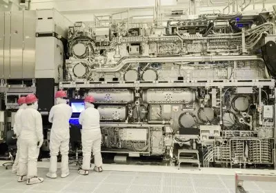
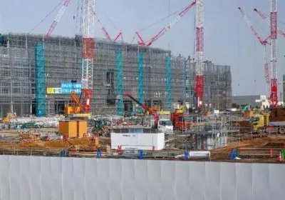
Ripple effect: While critics and PC enthusiasts are cheering for the AI bubble to burst, Big Tech and enterprise ventures cannot buy AI accelerators fast enough. In fact, even one of the world's most important chip manufacturers is now facing significant issues with its ability to meet customer demand.