Intel and Micron are announcing today that its joint venture company, IM Flash Technologies, is ready to sample the first 25nm NAND-based flash memory technology. In fewer words, that is the smallest semi-conductor process in the world.
The story broke earlier than anticipated during the weekend but the fact remains unchanged, flash memory using this new 25nm technology has roughly twice the density of a 34nm part at the same size. Manufacturers can take advantage of this reducing chip count by half, putting together a 256GB SSD with 32 chips instead of 64.

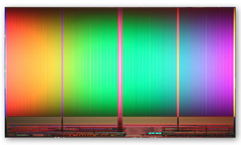
IMFT 25nm process NAND flash die
If you ever wondered why solid-state storage pricing dropped so dramatically over the last couple of years, NAND flash's lower density is the answer. IMFT was formed back in 2006 when they began sampling memory using a 72nm process. By 2008 they had moved to 40nm which is what the original Intel X25-M SSD utilized, and most recently 34nm in the second generation drives.
The first ever 25nm product is a 8GB die using 2-bits per cell MLC NAND flash (see the photo above) measuring a mere 167 sq. millimeters, or in more practical terms small enough to fit through the central hole of a CD while having 10+ times the data capacity. Intel expects consumer products based on 25nm NAND flash technology to become available before the end of the year.